


- PEO1: Graduates will develop strong foundations in VLSI design, semiconductor technology, and embedded systems, applying their knowledge to create innovative, efficient, and industry-relevant electronic solutions.
- PEO2: Graduates will continuously enhance their skills in emerging domains such as AI, Machine Learning, and advanced EDA tools in Semiconductor domain, ensuring adaptability to evolving technologies and global industry demands.
- PEO3: Graduates will demonstrate leadership, teamwork, and entrepreneurial abilities while upholding professional ethics, contributing to sustainable and socially relevant advancements in electronics and VLSI technology.
- PO1: Engineering Knowledge: Apply knowledge of mathematics, natural science, computing, engineering fundamentals and an engineering specialization to develop the solution of complex engineering problems.
- PO2: Problem Analysis: Identify, formulate, review research literature and analyze complex engineering problems reaching substantiated conclusions with consideration for sustainable development.
- PO3: Design/Development of Solutions: Design creative solutions for complex engineering problems and design/develop systems/components/processes to meet identified needs with consideration for public health and safety, whole-life cost, net zero carbon, culture, society, and environment as required.
- PO4: Conduct Investigations of Complex Problems: Conduct investigations of complex engineering problems using research-based knowledge including design of experiments, modelling, analysis & interpretation of data to provide valid conclusions.
- PO5: Engineering Tool Usage: Create, select and apply appropriate techniques, resources and modern engineering & IT tools, including prediction and modelling recognizing their limitations to solve complex engineering problems.
- PO6: The Engineer and The World: Analyze and evaluate societal and environmental aspects while solving complex engineering problems for its impact on sustainability with reference to economy, health, safety, legal framework, culture, and environment.
- PO7: Ethics: Apply ethical principles and commit to professional ethics, human values, diversity and inclusion; adhere to national & international laws.
- PO8: Individual and Collaborative Teamwork: Function effectively as an individual, and as a member or leader in diverse/multi-disciplinary teams.
- PO9: Communication: Communicate effectively and inclusively within the engineering community and society at large, such as being able to comprehend and write effective reports and design documentation, make effective presentations considering cultural, language, and learning differences.
- PO10: Project Management and Finance: Apply knowledge and understanding of engineering management principles and economic decision-making and apply these to one’s own work, as a member and leader in a team, and to manage projects and in multidisciplinary environments.
- PO11: Life-Long Learning: Recognize the need for, and have the preparation and ability for i) independent and life-long learning ii) adaptability to new and emerging technologies and iii) critical thinking in the broadest context of technological change.
- PSO1: Ability to apply advanced concepts of analog/digital CMOS design, ASIC/FPGA design flows, and hardware description languages (Verilog/SystemVerilog) to design, simulate, and verify integrated circuits using industry-standard EDA and CAD tools.
- PSO2:Understanding of semiconductor fabrication processes, testing methodologies, and packaging technologies.


Toastmasters Club
III Year ECE Students
Winners of Rockstar @ Toastmasters Club
Volkswagen imbiothon 2025
III Year ECE StudentS
Selected Top 10 in Volkswagen imbiothon 2025
Smart India Pitch Award
III Year ECE StudentS
Winners of Smart India Pitch Award
NXP Woman in Tech Program
II Year ECE Student
Among 75 Student Nationwide for the Prestigious NXP Woman in Tech Program
Samartha
III Year ECE Students
4rd place of Samartha – 36 Hours National Level Hackathon
Semester - Long Internship, IIT Bombay
II Year ECE Students
Successfully completed a semester-long internship at IIT Bombay.
MeitY Grand Challenge 2024
III Year ECE Students
One among the Top 10 Finalist MGC 24
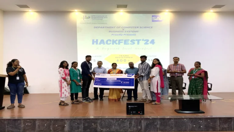
HackFest 2024
IV Year ECE Students
Won 2nd Prize with Rs. 10,000 Cash award
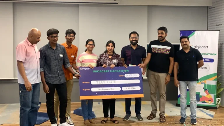
36 hours NinjaCart Hackathon
IV Year ECE Students
Won 2nd Prize with Rs. 50,000 Cash award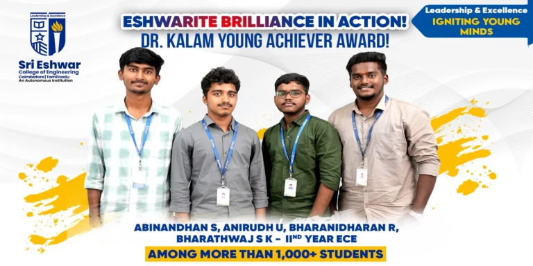
Dr.Kalam Young Achiever Award
II Year ECE Students
Among More than 1000+ Students

December 15 - 27, 2025
Internship in Analog and Digital IC Design

September 15, 2025
Simulathon

September 12, 2025
Recent Trends in VLSI Design

September 12 - 15, 2025
Simulathon

July 24, 2025
Electronics Engineers : Skills and Readiness For Emerging Roles in the Automotive Industry

July 07 - 11, 2025
Circuit Analysis, Semiconductor Devices & Electronic Circuits

July 02 - 19, 2025
Hal, Bare Metal Programming And Rtos

June 02 & -06, 2025
Advanced Embedded System Design and Industrial Automation

May 14 & -15, 2025
Python Django Meets Mongo DB

June 16-21, 2025
FDP on Embedded and IOT

June 09, 2025
Evolving Technologies in Contemporary Defence and Aerospace Systems and Holistic insight into Relevant Electronic and Communication Systems Engineering

May 03, 2025
Workshop on Embedded IOT for Breakthrough Innovation

Mar 06,07 & 10, 2025
Hands on session on Intel 8051 and it’s Applications

Mar 08, 2025
Seminar on Job Opportunities in Embedded Systems& Semiconductor Manufacturing

Feb 17 , 2025
FDP on Wearable Electronics for Biomedical Applications

Feb 17 , 2025
FDP on Wearable Electronics for Biomedical Applications

Dec 21 , 2024
Breaking Barriers organized by WWC and Posh Cell

Oct 07 & 08, 2024
Advanced Problem -Solving Techniques in Smart Phones

Aug 24 , 2024
Leadership Talk on VLSI Day

Aug 29 - 30 , 2024
Hands-on Training in NETSIM

July 29 - 14 Aug, 2024
Augmented Reality Virtual Reality

July 22 - 26 Sep, 2024
RTL Design and Verification

July 15 - 19 July, 2024
Unified Approaches to digital system architecture and signal processing

July 22 - 26 July, 2024
Smart Solutions Bridging Embedded System IOT and MICROPROCESSOR ELECTRONICS

July 29 - 14 Aug, 2024
Organizes Summer Internship on Demystifying Networking


Sophisticated infrastructure, including state-of-the-art labs, enhanced my educational experience
Dhanush M
2017, Tech Mahindra

Innovative management practices ensured a seamless and enriching academic experience.
Karunakar Rao
2013, Akamai Technologies

Effective placement programs at Sri Eshwar were critical in securing prestigious job offers
Krishnaprasad R
2017, Harman

Management's strategic initiatives significantly improved the quality of education and student life.
Maneesh Sharma
2016, Aisera

Proactive management ensured a dynamic and engaging academic atmosphere
Mukundhan G
2016, Bosch Global Software Technologies


